CDCLVC11xx 3.3-V and 2.5-V LVCMOS High-Performance Clock Buffer Family
一、CDCLVC1104时钟clock buffer产品特点:
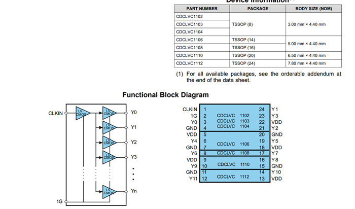
1• High-Performance 1:2, 1:3, 1:4, 1:6, 1:8, 1:10, 1:12 LVCMOS Clock Buffer Family
• Very Low Pin-to-Pin Skew < 50 ps • Very Low Additive Jitter < 100 fs
• Supply Voltage: 3.3 V or 2.5 V
• fmax = 250 MHz for 3.3 V fmax = 180 MHz for 2.5 V
• Operating Temperature Range: –40°C to 85°C
• Available in 8-, 14-, 16-, 20-, 24-Pin TSSOP Package (All Pin-Compatible)
二、CDCLVC1104时钟clock buffer产品就用
Applications General-Purpose Communication, Industrial, and Consumer Applications
三、CDCLVC1104时钟clock buffer特性
Description The CDCLVC11xx is a modular, high-performance, low-skew, general-purpose clock buffer family from Texas Instruments.
The entire family is designed with a modular approach in mind. It is intended to round up TI's series of LVCMOS clock generators.
Seven different fan-out variations, 1:2 to 1:12, are available. All of the devices are pin-compatible to each other for easy handling.
All family members share the same high performing characteristics such as low additive jitter, low skew, and wide operating temperature
range.
The CDCLVC11xx supports an asynchronous output enable control (1G) which switches the outputs into a low state when 1G is low.
The CDCLVC11xx family operates in a 2.5-V and 3.3-V environment and are characterized for operation from –40°C to 85°C.
TI德州仪器代理商华芯旺提供时钟发生器,时钟buffer,PCIE时钟发生器,RTC,电平转换芯片,CDCLVC1104时钟clock buffe,
CDCLVC1104国产兼容替产找华芯旺科技索取资料及样片13923807831.